
FPGA-based development differs from traditional embedded programming, offering companies the ability to create unique hardware architectures tailored to specific computational tasks. However, high development costs and a shortage of skilled engineers eventually force businesses to make trade-offs regarding process flexibility, given the performance constraints of the logic.
What Makes FPGA Development Different From Embedded Software Design
Let’s define the main embedded software vs FPGA difference.
Core Architecture: Programmable Logic vs. Fixed Processor Cores
The main difference between FPGAs and microcontrollers/microprocessors lies at the hardware level: while embedded systems involve writing code to run on a specific processor architecture – featuring a predefined instruction set, ALUs, and a register file (with instructions executed sequentially) – FPGA development entails designing the physical hardware itself. The FPGA architecture consists of a matrix of configurable logic blocks, embedded memory, digital signal processors, and programmable I/O blocks.
It is important to note that coding for such projects is done using hardware description languages ; the engineer’s task is to define how logic gates and flip-flops are physically interconnected within the chip. In other words:
- In embedded software, optimization covers execution flow, processor cycles, memory/power consumption, and so on.
- In FPGA development, optimization focuses on chip topology, critical paths, timing closure, and resource routing.
Parallelism in FPGA Programming vs. Sequential Execution in Microcontrollers
Even multi-core processors execute instructions sequentially. When parallelism is required, RTOS, interrupts, and multithreading come into play. However, at the level of a single processor core, execution remains pipelined and sequential. As the workload increases, this inevitably leads to latency and timing instability.
In this context, FPGAs provide true hardware parallelism: each function defined in the logic is allocated its own isolated area on the chip and operates independently of the other elements.
For instance, if you need to process 32 high-speed digital channels simultaneously, an FPGA will run 32 parallel hardware computing units without time penalties or forced prioritization – simply because the system's performance scales through an increase in the physical volume of the chip's logic resources.
Main Drivers Behind Choosing FPGA Design and Development
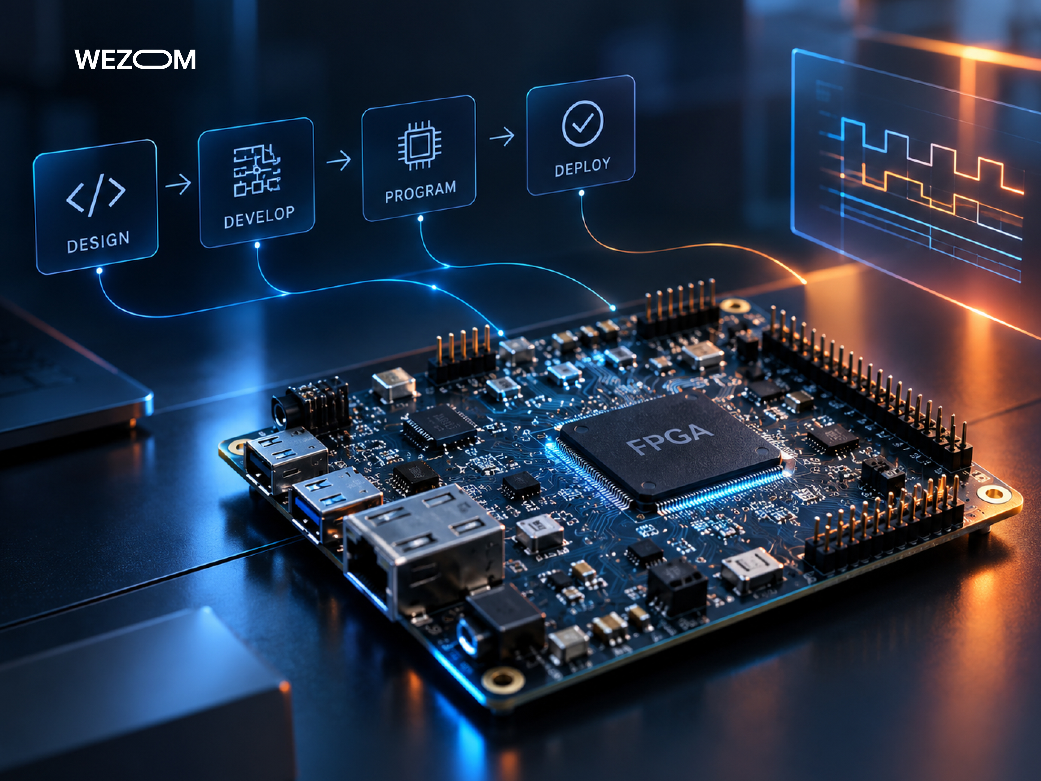
For applications requiring response predictability that meets hard real-time standards, standard microcontrollers are unsuitable due to delays caused by OS context switching, software interrupt processing, data bus latency, and the like.
Real-Time Processing and Ultra-Low Latency Requirements
FPGA design and development enable on-the-fly data processing – that is, without loading data into external memory or using command queues. This is achieved through:
- Determinism, where the signal processing time from input to output is fixed and determined by the propagation delay through logic gates;
- Ultra-low latency, where the response to an event takes mere nanoseconds;
- The absence of jitter, as the logic operates based on a clock signal, ensuring consistent timing characteristics.
Custom Hardware Acceleration for Signal and Image Processing
Tasks requiring the continuous execution of repetitive operations on large datasets (such as digital signal processing, Fast Fourier Transforms, Kalman filtering, cryptographic encryption, and the like) quickly exhaust the resources of general-purpose processors. This is where hardware acceleration through the FPGA comes into play, handling these tasks via specialized hardware accelerators that rely on:
- Pipelining, where the algorithm is broken down into physical stages, with each stage executed in a single clock cycle;
- Embedded DSP blocks, operating at frequencies of hundreds of megahertz, providing immense computational power by default.
Long-Term Flexibility Through Hardware Reconfiguration
Unlike ASICs, the development of which costs millions of dollars and offers no possibility of correcting errors once implemented, the FPGA supports in-system reconfiguration, providing businesses with the following advantages:
- Protection against obsolescence (meaning that if industry standards or communication protocols change, an FPGA-based device can be updated remotely by uploading a new binary file);
- Reduced time-to-market (allowing you to launch with basic functionality and subsequently update the logic at the customer's site);
- Platform unification (where a single hardware module can perform different functions depending on the loaded firmware, thereby minimizing PCB design and supply chain costs).
FPGA Programming Languages and Toolchains Explained
Choosing between the programmable logic design and a microcontroller architecture based on embedded software always comes down to balancing performance, time-to-market, and the project budget. Specifically, FPGA development requires a highly specialized tech stack, whereas an RTOS-based software approach is optimal when budget savings and ease of debugging are priorities.
VHDL vs. Verilog vs. SystemVerilog: Choosing an FPGA Programming Language
In standard programming, code is executed sequentially by a processor, whereas hardware description languages are used to model and synthesize digital electronic circuits. Here are the most popular FPGA programming languages:
- VHDL, which was developed at the behest of the US Department of Defense. It is a strongly typed FPGA programming language that minimizes the risk of hidden errors during compilation, though its syntax can often be verbose. It is frequently used in the aerospace, defense, and healthcare industries.
- Verilog, a commercial modeling C-like syntax language. It is less strict regarding data types and enables writing concise code in the context of the VHDL vs Verilog dilemma (though this can lead to difficulties for the inexperienced, as one might inadvertently describe an unwanted flip-flop or combinational loop that gets interpreted differently than intended).
- SystemVerilog, which combines RTL structure description capabilities with object-oriented extensions for verification. It enables the creation of complex testbenches, the measurement of test coverage, and much more.
High-Level Synthesis (HLS) and C/C++-to-RTL Workflows
The FPGA process involves writing RTL code by hand. The high-level synthesis (HLS) technology was developed to reduce the time required for this task – it enables the translation of algorithms written in high-level languages into RTL descriptions in VHDL/Verilog.
In this workflow, the developer first describes the algorithm in C/C++ using pragmas; the HLS compiler then analyzes the data dependency graph, automatically scheduling operations across clock cycles and allocating them to chip resources. This approach accelerates the programming process by a factor of 3 to 5 and allows for the rapid testing of architectural solutions, including the potential integration of libraries (such as OpenCV) or mathematical functions directly into the logic.
While this approach is excellent for computational tasks, it is inefficient for developing control logic and low-level bus controllers.
Popular FPGA Development Boards and Vendor Ecosystems (Xilinx, Intel/Altera, Lattice)
The FPGA market is divided among several players, including:
- AMD Xilinx. Main product families are Artix-7/Spartan-7/Kintex-7/Kintex UltraScale/Virtex UltraScale+/Zynq-7000/Zynq MPSoC. Regarding tools, the Vivado Design Suite (an environment for synthesis/place-and-route/debugging) and Vitis (an environment for heterogeneous computing and HLS) are noteworthy. Notable development boards include the Digilent Arty A7/Zybo Z7/Kria SOM.
- Intel FPGA. Within this brand, the Cyclone IV/Cyclone 10/Arria 10/Stratix 10/Agilex families, the Intel Quartus Prime and Qsys tools, and development boards such as the DE10-Lite and Terasic DE10-Nano are particularly noteworthy.
- Lattice Semiconductor. The iCE40/CrossLink/MachXO3/MachXO5 families, tools such as Lattice Diamond/Radiant, and open-source compilers like Yosys/IceStorm deserve attention here.
Embedded Software Development: Strengths and Practical Limits
Despite the real-time processing FPGA, developing RTOS embedded systems remains the optimal choice for the vast majority of commercial applications.
When Microcontrollers and RTOS-Based Systems Are the Better Fit
Using microcontrollers makes sense in the following cases:
- Complex decision-making logic, for instance, when a device must simultaneously handle text menus, manage file systems, support multiple network protocols, and host a web server;
- Relaxed requirements for parallelism and latency – specifically, scenarios where sensor sampling rates do not exceed hundreds of kilohertz and event response times in the low-millisecond range are sufficient;
- Standard communication interfaces (such as UART/SPI/I2C/CAN/USB/Ethernet), implemented as hardware blocks that are activated by initializing a few registers.
Cost, Power, and Time-to-Market Trade-Offs vs. FPGA Design
Three factors are important when considering the FPGA vs microcontroller choice:
- Component cost. When using MCUs, the choice typically involves mass-produced solutions (such as 32-bit STM32 chips) costing between $0.50 and $10 per unit. In contrast, FPGA chips start at $15 and can exceed $10,000 per unit; additionally, this approach necessitates the use of PMICs with multiple power rails and multi-layer printed circuit boards.
- Power consumption/heat dissipation. Microcontrollers are optimized for energy efficiency and support deep-sleep modes, often allowing them to operate for years on a single battery. Conversely, the FPGA approach involves transistor switching within the matrix on every clock cycle, resulting in significant power consumption (ranging from several watts to tens of watts) and requiring active cooling.
- Time-to-market. When opting for an MCU, code is written in C/C++ and compiles in seconds (with debugging performed via the SWD/JTAG interface in step-by-step mode). In contrast, with an FPGA, the project build process can take several hours – all without the benefit of step-by-step debugging (engineers must run simulations instead).
Ultimately, the choice comes down to a dilemma: if a task can be efficiently handled in software on a microcontroller or general-purpose processor without violating strict timing constraints, a software-based approach is preferable; however, if the physical limitations of sequential processors pose an obstacle, then developing for an FPGA makes sense.
Decision Framework: FPGA Development vs. Embedded Software by Use Case
When designing the architecture of an electronic device, another question always arises: is it possible to rely on a software-based solution using an off-the-shelf processor, or is it necessary to design a custom chip? Making the wrong choice leads either to budget overruns on components and missed deadlines or to an inability to meet technical requirements regarding performance or latency.
Industrial Automation, Aerospace, and Defense Applications
In industrial systems, main factors include deterministic timing, hardware fault tolerance, and real-time event response. For instance, controlling high-power inverters or grid protection relays requires microsecond-level response times; here, the FPGA enables the implementation of real-time parallel control loops, even under heavy operating system loads. The aerospace and defense sectors are also worth considering, as they require the real-time parallel processing of hundreds of digital channels, and FPGA programming eliminates failures caused by software thread hangs.
Telecommunications, 5G, and High-Speed Data Interfaces
Telecommunications require a PHY layer capable of immediate response. In the context of 5G, for instance, base stations take on beamforming, digital signal processing, etc. – all at speeds reaching 10+ gigabits per second. It becomes evident why standard microcontrollers cannot handle such data throughput. The same applies to 100G/400G routers, which must utilize SERDES transceivers integrated into the FPGA. This allows programmable logic to handle packet filtering/routing, ensuring zero frame loss.
Medical Devices, Robotics, and Edge AI Inference
In medical equipment sectors, the parallel system determinism and the real-time streaming video processing become main requirements. For instance, ultrasound and tomography systems require the initial cleaning and filtering of signals from hundreds of sensors; here, the FPGA acts as hardware signal accelerators prior to data transmission for visualization. Regarding industrial manipulators and, for example, surgical robots, these systems rely on the synchronous control of dozens of servo drives using protocols such as EtherCAT/PROFINET IRT. In such systems, the FPGA eliminates phase shift, ensuring an instantaneous feedback response. Finally, regarding edge AI FPGA: for AI deployment on drones, the FPGA can deliver low energy consumption per inference while maintaining fixed frame latency – capabilities that mobile GPUs lack.
Hybrid Architectures: Combining FPGA Programming With Embedded Software
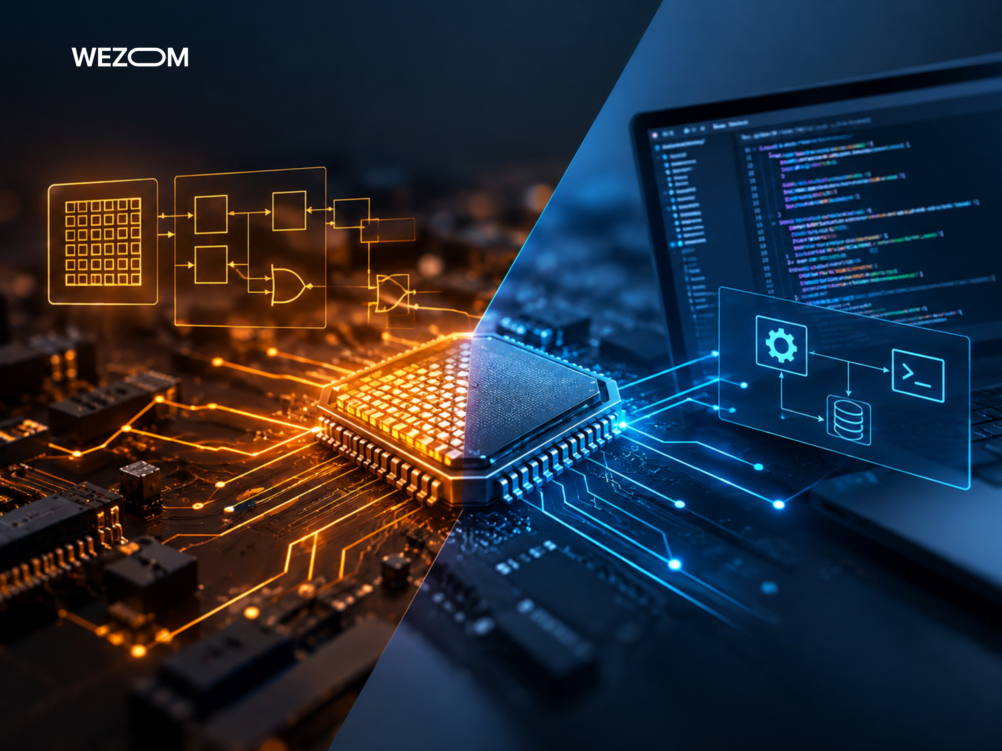
Attempting to implement the device's entire functionality within an FPGA unnecessarily complicates the design. In this regard, the best modern solutions rely on hybrid architectures, where each hardware element performs the specific task for which it was originally best suited.
SoC FPGAs and ARM Co-Processor Integration
SoC FPGA families (such as AMD Xilinx Zynq or Intel Cyclone V) have radically transformed embedded system design. A single chip now consolidates a processing system (a hardware subsystem based on multi-core ARM processors with built-in DDR/Ethernet memory controllers and peripherals), programmable logic, and a high-bandwidth bus (typically based on the ARM AMBA AXI4 standard). This enables the transfer of data arrays between the logic and the processor's RAM via direct memory access with nanosecond-level latency.
Firmware-to-Hardware Partitioning Strategies
The primary task for a hybrid system designer is to determine which functions are best implemented in software and which in hardware. Typically, high-level tasks (such as the graphical user interface, cloud interaction via MQTT/HTTP, file system management, access control, software updates, and slow control routines) are assigned to the software component. Conversely, latency-sensitive algorithms (including initial signal filtering, stream encryption, hardware video codecs, checksum calculation, PWM signal generation, and non-standard data transmission protocols) are handled by the hardware.
Best Practices for FPGA Design and Development Success
FPGA development should not rely on ad-hoc algorithms. The issue is that, in standard programming, any error can be debugged and fixed in a couple of minutes, whereas a poorly designed FPGA topology can lead to weeks of tedious troubleshooting to determine why the system isn't behaving as originally intended.
Simulation, Verification, and Timing Closure
Our experience shows that the "right" foundation for an FPGA project rests on three pillars:
- Intensive behavioral simulation. This means that before the firmware is loaded onto the physical chip, the RTL code must achieve 100% test coverage. Verification frameworks come into play here, enabling millions of random input data combinations to be fed into the virtual circuit to identify boundary conditions and signal race conditions.
- Static timing analysis. Unlike conventional programming, FPGA logic is constrained by the physical laws governing electrical signal propagation through silicon. This is why an engineer must initially specify timing constraints (including clock frequencies, I/O pin delays, etc.).
- Timing closure. This refers to optimizing code and routing settings to eliminate setup and hold time violations. In other words, if the signal's electrical edge fails to reach the flip-flop within a single clock cycle, the circuit will produce unpredictable results.
Common Pitfalls When Migrating From Software to FPGA Programming
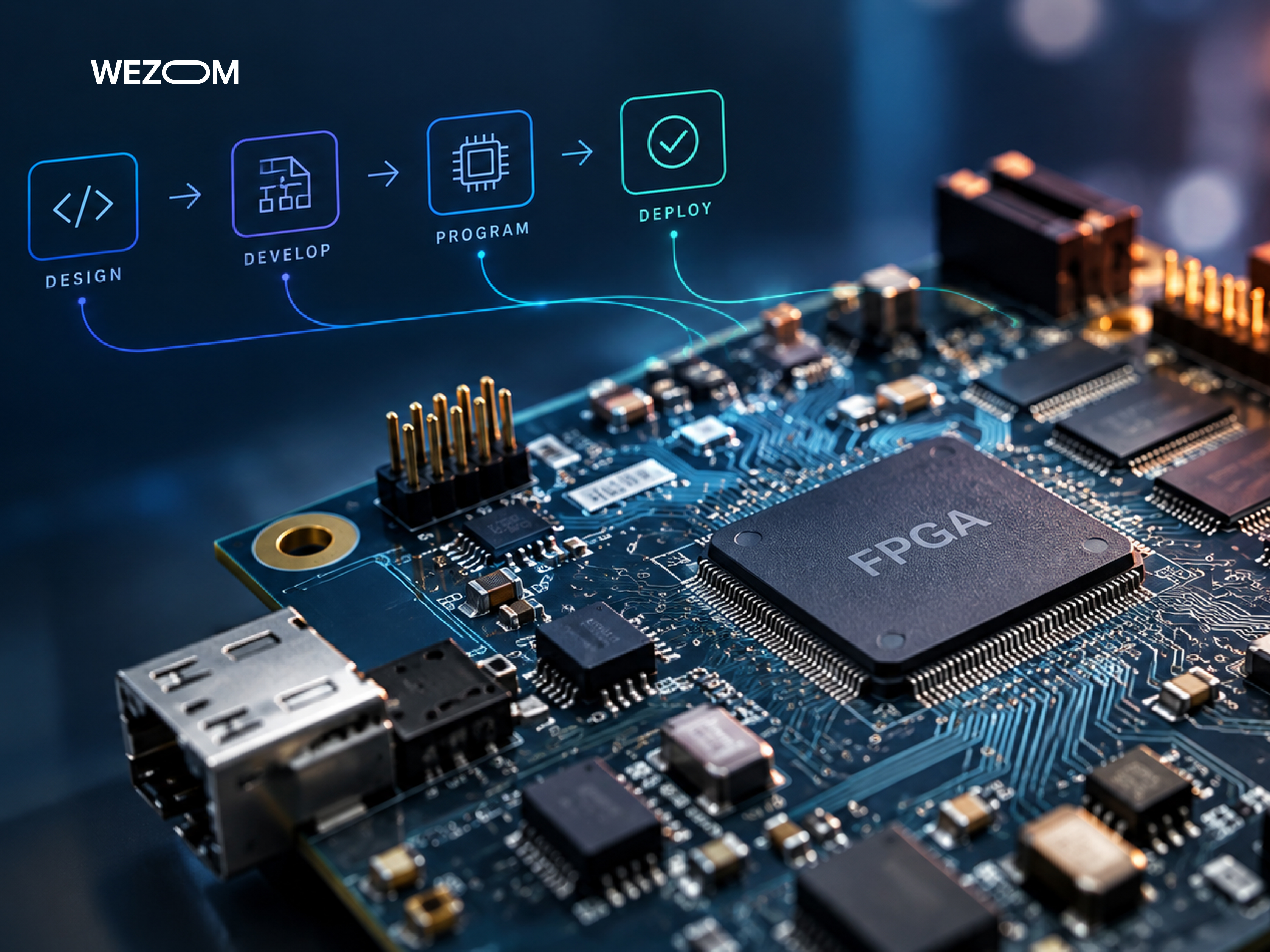
Engineers with a background in conventional programming who are new to VHDL or Verilog often encounter the following conceptual pitfalls regarding implementation:
- Writing RTL code as a sequential algorithm. In HDL, listing statements one after another does not imply sequential execution; constructs outside of process blocks execute concurrently and without interruption.
- Ignoring chip resources. A developer might describe the division of two 64-bit floating-point numbers in a single line of code. Consequently, the synthesis tool will attempt to generate a massive combinational circuit that completely exhausts the FPGA development board's resources.
- Creating unintended latches. If not all possible signal states are covered within a combinational `if-else`/`case` block, the compiler is forced to latch the previous value, creating clock-related issues.
- Inability to deal with clock domains. This covers data transfer between blocks driven by clock sources only (i.e., without synchronization). Such practices lead to sporadic glitches, though the issue can be resolved with two-flip-flop synchronizers.
FAQ
How much does FPGA development typically cost compared to embedded software projects?
FPGA development costs, on average, two to five times more than standard embedded software development; this is due to a significantly longer verification cycle, simulation complexity, and the high hourly rates of HDL engineers. It is also important to consider the cost of the FPGA chips themselves (ranging from $30 to over $3,000) which far exceeds the price of microcontrollers, typically costing between $1 and $15.
What skills or background are needed to start learning FPGA programming?
Requirements include knowledge of digital circuit design, an understanding of physical fundamentals (including clock domains and critical paths), and proficiency in HDL languages.
Can FPGA designs be updated in the field after deployment, like software firmware?
Yes, they can. Just like a microcontroller's firmware, an FPGA bitstream can be updated either over-the-air or via SPI/JTAG interfaces, allowing a new hardware configuration to be loaded into non-volatile memory without the need to replace the chip.
How does power consumption compare between FPGAs and embedded microcontrollers?
Microcontrollers are optimized for low power consumption and support deep-sleep modes. Due to their extensive interconnect matrices, FPGAs consume anywhere from hundreds of milliwatts to tens of watts and generate significant heat.
What is the typical learning curve for engineers moving from embedded software to FPGA design and development?
The learning curve is steep, as specialists must shift their mindset from sequential code execution to parallel hardware circuitry. More precisely, the transition from writing C code to HDL development typically takes an engineer between 6 and 12 months.
Are there open-source tools available for FPGA programming, or is it vendor-locked?
Traditionally, the industry has been tied to proprietary CAD tools (such as AMD Vivado or Intel Quartus); however, an open-source ecosystem stack (Yosys+NextPNR+IceStorm) is now emerging for low-cost chips (like the Lattice iCE40 and ECP5), making it possible to implement projects without vendor-specific software.
How do you decide between an FPGA, an ASIC, and a standard microcontroller for a new product?
Microcontrollers are characterized by low cost, standard interfaces, sequential tasks, and low computational loads, whereas FPGAs require ultra-low latency (under 100 ns), parallel DSP capabilities, flexibility, and suitability for small-to-medium production runs. ASICs, on the other hand, are intended for high-volume production (hundreds of thousands of units), where a compact form factor, minimal unit cost, and maximum energy efficiency are critical.
